Wednesday, 29/04/2026 | 20:39 GMT+7
Researchers in The Edward S. Rogers Sr. Department of Electrical & Computer Engineering used this insight to invent something totally new: they've combined two promising solar cell materials together for the first time, creating a new platform for LED technology.
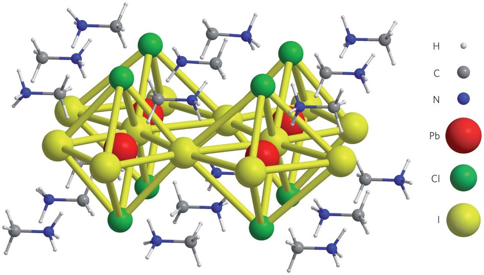
The team designed a way to embed strongly luminescent nanoparticles called colloidal quantum dots (the chocolate chips) into perovskite (the oatmeal cookie). Perovskites are a family of materials that can be easily manufactured from solution, and that allow electrons to move swiftly through them with minimal loss or capture by defects.
The work is published in the international journal Nature on July 15, 2015.
"It's a pretty novel idea to blend together these two optoelectronic materials, both of which are gaining a lot of traction," says Xiwen Gong, one of the study's lead authors and a PhD candidate working with Professor Ted Sargent. "We wanted to take advantage of the benefits of both by combining them seamlessly in a solid-state matrix."
The result is a black crystal that relies on the perovskite matrix to 'funnel' electrons into the quantum dots, which are extremely efficient at converting electricity to light. Hyper-efficient LED technologies could enable applications from the visible-light LED bulbs in every home, to new displays, to gesture recognition using near-infrared wavelengths.
"When you try to jam two different crystals together, they often form separate phases without blending smoothly into each other," says Dr. Riccardo Comin, a post-doctoral fellow in the Sargent Group. "We had to design a new strategy to = convince these two components to forget about their differences and to rather intermix into forming a unique crystalline entity."

The main challenge was making the orientation of the two crystal structures line up, called heteroexpitaxy. To achieve heteroepitaxy, Gong, Comin and their team engineered a way to connect the atomic 'ends' of the two crystalline structures so that they aligned smoothly, without defects forming at the seams. "We started by building a nano-scale scaffolding 'shell' around the quantum dots in solution, then grew the perovskite crystal around that shell so the two faces aligned," explained coauthor Dr. Zhijun Ning, who contributed to the work while a post-doctoral fellow at UofT and is now a faculty member at ShanghaiTech.
The resulting heterogeneous material is the basis for a new family of highly energy-efficient near-infrared LEDs. Infrared LEDs can be harnessed for improved night-vision technology, to better biomedical imaging, to high-speed telecommunications.
Combining the two materials in this way also solves the problem of self-absorption, which occurs when a substance partly re-absorbs the same spectrum of energy that it emits, with a net efficiency loss. "These dots in perovskite don't suffer reabsorption, because the emission of the dots doesn't overlap with the absorption spectrum of the perovskite," explains Comin.
Gong, Comin and the team deliberately designed their material to be compatible with solution-processing, so it could be readily integrated with the most inexpensive and commercially practical ways of manufacturing solar film and devices. Their next step is to build and test the hardware to capitalize on the concept they have proven with this work.
"We're going to build the LED device and try to beat the record power efficiency reported in the literature," says Gong.
This work was supported by the Ontario Research Fund Research Excellence Program, the Natural Sciences and Engineering Research Council of Canada (NSERC), and the King Abdullah University of Science & Technology (KAUST).
Anh Tuan


 Prime Minister Issues Directive to Strengthen Electricity Saving and Promote Rooftop Solar Power Development
07/04/2026
 Large-Space Cooling Solution Helps Achieve Up to 36% Annual Energy Savings
 Energy Manager Training Course in Ho Chi Minh City
 Launch of energy manager training courses in Hanoi and Ho Chi Minh City
 Strict and Effective Implementation of the VNEEP3
 Thai Nguyen Enterprises Save Energy for Sustainable Growth
 Launch of energy manager training courses (May) in Hanoi and Ho Chi Minh City
 Hanoi Implements the 2026 Plan on Energy Efficiency and Conservation